 국립중앙도서관 "우편 복사 서비스"로 연결 됩니다.


 ScienceON
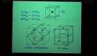
Graphite/Ni composite films have been deposited on SiO<SUB>2</SUB>/Si (100) wafers by varying their graphite concentration (<I>n</I><SUB>G</SUB>) and thickness (t) from 2 to 12 wt % and 40 to 400 nm, respectively in...
다국어 입력
あ
ぁ
か
が
さ
ざ
た
だ
な
は
ば
ぱ
ま
や
ゃ
ら
わ
ゎ
ん
い
ぃ
き
ぎ
し
じ
ち
ぢ
に
ひ
び
ぴ
み
り
う
ぅ
く
ぐ
す
ず
つ
づ
っ
ぬ
ふ
ぶ
ぷ
む
ゆ
ゅ
る
え
ぇ
け
げ
せ
ぜ
て
で
ね
へ
べ
ぺ
め
れ
お
ぉ
こ
ご
そ
ぞ
と
ど
の
ほ
ぼ
ぽ
も
よ
ょ
ろ
を
ア
ァ
カ
サ
ザ
タ
ダ
ナ
ハ
バ
パ
マ
ヤ
ャ
ラ
ワ
ヮ
ン
イ
ィ
キ
ギ
シ
ジ
チ
ヂ
ニ
ヒ
ビ
ピ
ミ
リ
ウ
ゥ
ク
グ
ス
ズ
ツ
ヅ
ッ
ヌ
フ
ブ
プ
ム
ユ
ュ
ル
エ
ェ
ケ
ゲ
セ
ゼ
テ
デ
ヘ
ベ
ペ
メ
レ
オ
ォ
コ
ゴ
ソ
ゾ
ト
ド
ノ
ホ
ボ
ポ
モ
ヨ
ョ
ロ
ヲ
―
http://chineseinput.net/에서 pinyin(병음)방식으로 중국어를 변환할 수 있습니다.
변환된 중국어를 복사하여 사용하시면 됩니다.
예시)
- 中文 을 입력하시려면 zhongwen을 입력하시고 space를누르시면됩니다.
- 北京 을 입력하시려면 beijing을 입력하시고 space를 누르시면 됩니다.
А
Б
В
Г
Д
Е
Ё
Ж
З
И
Й
К
Л
М
Н
О
П
Р
С
Т
У
Ф
Х
Ц
Ч
Ш
Щ
Ъ
Ы
Ь
Э
Ю
Я
а
б
в
г
д
е
ё
ж
з
и
й
к
л
м
н
о
п
р
с
т
у
ф
х
ц
ч
ш
щ
ъ
ы
ь
э
ю
я
′
″
℃
Å
¢
£
¥
¤
℉
‰
$
%
F
₩
㎕
㎖
㎗
ℓ
㎘
㏄
㎣
㎤
㎥
㎦
㎙
㎚
㎛
㎜
㎝
㎞
㎟
㎠
㎡
㎢
㏊
㎍
㎎
㎏
㏏
㎈
㎉
㏈
㎧
㎨
㎰
㎱
㎲
㎳
㎴
㎵
㎶
㎷
㎸
㎹
㎀
㎁
㎂
㎃
㎄
㎺
㎻
㎽
㎾
㎿
㎐
㎑
㎒
㎓
㎔
Ω
㏀
㏁
㎊
㎋
㎌
㏖
㏅
㎭
㎮
㎯
㏛
㎩
㎪
㎫
㎬
㏝
㏐
㏓
㏃
㏉
㏜
㏆

RISS 인기검색어
https://www.riss.kr/link?id=A104203148
-
저자
신동희 (경희대학교) ; Seung Bum Yang (Kyung Hee University) ; Dong Yeol Shin (Kyung Hee University) ; 김창오 (경희대학교) ; 김성 (경희대학교) ; 최석호 (경희대학교) ; 백상현 (경희대학교)
- 발행기관
- 학술지명
- 권호사항
-
발행연도
2012
-
작성언어
English
-
주제어
Graphene ; Graphite ; Ni ; Sputtering
-
등재정보
KCI등재,SCI,SCIE,SCOPUS
-
자료형태
학술저널
-
수록면
563-567(5쪽)
-
KCI 피인용횟수
2
- 제공처
-
0
상세조회 -
0
다운로드
부가정보
다국어 초록 (Multilingual Abstract)
Graphite/Ni composite films have been deposited on SiO<SUB>2</SUB>/Si (100) wafers by varying their graphite concentration (<I>n</I><SUB>G</SUB>) and thickness (t) from 2 to 12 wt % and 40 to 400 nm, respectively in a RF sputtering system, subsequently annealed at 900 ℃ for 4 min, and then slowly cooled to room temperature to form graphene layer on Ni surface. Several structural-analysis techniques reveal optimum <I>n</I><SUB>G</SUB> (~8 wt %) and t (~160 nm) of the composite films for the synthesis of fewest-layer and defect-minimized graphene. At the annealing temperature, carbon atoms diffuse out from the composite film followed by their precipitation as graphene on the Ni layer as the carbon solubility limit in Ni is reached during the cooling period. Based on this mechanism, the optimum conditions are explained. Our approach provides advantages to tune the number of layers simply by varying <I>n</I><SUB>G</SUB> and t of the composite films.
참고문헌 (Reference)
1 A. K. Geim, 6 : 183-, 2007
2 Z-S. Wu, 47 : 493-, 2009
3 K. S. Kim, 457 : 706-, 2009
4 K. S. Novoselov, 438 : 197-, 2005
5 Y. B. Zhang, 438 : 201-, 2005
6 K. S. Novoselov, 306 : 666-, 2004
7 B. Partoens, 74 : 075404-, 2006
8 X. Li, 324 : 1312-, 2009
9 A. Reina, 9 : 30-, 2009
10 R. Kikowatz, 5 : 1009-, 1987
11 J. B. Oostinga, 7 : 151-, 2008
12 M. Zheng, 96 : 063110-, 2010
13 S. Garaj, 97 : 183103-, 2010
14 Y. Zhang, 459 : 820-, 2009
15 Q. Yu, 93 : 113103-, 2007
16 A. Gupta, 6 : 2667-, 2006
17 A. C. Ferrari, 97 : 187401-, 2006
18 D. Graf, 7 : 238-, 2007
19 S. Chen, 11 : 3519-, 2011
20 F. Giannazzo, 7 : 1251-, 2010
21 Do Kyu Lee, "Annealing Effect on the Electrical and the Optical Characteristics of Undoped ZnO Thin Films Grown on Si Substrates by RF Magnetron Sputtering" 한국물리학회 51 (51): 1378-1382, 2007
동일학술지(권/호) 다른 논문
-
- 한국물리학회
- Seong Kyu Seo
- 2012
- KCI등재,SCI,SCIE,SCOPUS
-
- 한국물리학회
- 김창오
- 2012
- KCI등재,SCI,SCIE,SCOPUS
-
- 한국물리학회
- Dongkyu Jeong
- 2012
- KCI등재,SCI,SCIE,SCOPUS
-
A Modified Iterative Algorithm for Phase Retrieval
- 한국물리학회
- 김우식
- 2012
- KCI등재,SCI,SCIE,SCOPUS
분석정보
인용정보 인용지수 설명보기
학술지 이력
| 연월일 | 이력구분 | 이력상세 | 등재구분 |
|---|---|---|---|
| 2023 | 평가예정 | 해외DB학술지평가 신청대상 (해외등재 학술지 평가) | |
| 2020-01-01 | 평가 | 등재학술지 유지 (해외등재 학술지 평가) |  |
| 2011-01-01 | 평가 | 등재학술지 유지 (등재유지) | |
| 2009-01-01 | 평가 | 등재학술지 유지 (등재유지) | |
| 2007-01-01 | 평가 | SCI 등재 (등재유지) | |
| 2005-01-01 | 평가 | 등재학술지 유지 (등재유지) | |
| 2002-07-01 | 평가 | 등재학술지 선정 (등재후보2차) | |
| 2000-01-01 | 평가 | 등재후보학술지 선정 (신규평가) |  |
학술지 인용정보
| 기준연도 | WOS-KCI 통합IF(2년) | KCIF(2년) | KCIF(3년) |
|---|---|---|---|
| 2016 | 0.47 | 0.15 | 0.31 |
| KCIF(4년) | KCIF(5년) | 중심성지수(3년) | 즉시성지수 |
| 0.26 | 0.2 | 0.26 | 0.03 |

이 자료와 함께 이용한 RISS 자료
나만을 위한 추천자료


