 국립중앙도서관 "우편 복사 서비스"로 연결 됩니다.

 KCI
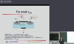
KCIAt nanoscale along with the failure of Metal oxide semiconductor field-effect transistor due to short channel effects, Silicon has raised as another bottleneck for researchers. In the last couple of decades, researchers have provided diff erent soluti...
다국어 입력
あ
ぁ
か
が
さ
ざ
た
だ
な
は
ば
ぱ
ま
や
ゃ
ら
わ
ゎ
ん
い
ぃ
き
ぎ
し
じ
ち
ぢ
に
ひ
び
ぴ
み
り
う
ぅ
く
ぐ
す
ず
つ
づ
っ
ぬ
ふ
ぶ
ぷ
む
ゆ
ゅ
る
え
ぇ
け
げ
せ
ぜ
て
で
ね
へ
べ
ぺ
め
れ
お
ぉ
こ
ご
そ
ぞ
と
ど
の
ほ
ぼ
ぽ
も
よ
ょ
ろ
を
ア
ァ
カ
サ
ザ
タ
ダ
ナ
ハ
バ
パ
マ
ヤ
ャ
ラ
ワ
ヮ
ン
イ
ィ
キ
ギ
シ
ジ
チ
ヂ
ニ
ヒ
ビ
ピ
ミ
リ
ウ
ゥ
ク
グ
ス
ズ
ツ
ヅ
ッ
ヌ
フ
ブ
プ
ム
ユ
ュ
ル
エ
ェ
ケ
ゲ
セ
ゼ
テ
デ
ヘ
ベ
ペ
メ
レ
オ
ォ
コ
ゴ
ソ
ゾ
ト
ド
ノ
ホ
ボ
ポ
モ
ヨ
ョ
ロ
ヲ
―
http://chineseinput.net/에서 pinyin(병음)방식으로 중국어를 변환할 수 있습니다.
변환된 중국어를 복사하여 사용하시면 됩니다.
예시)
- 中文 을 입력하시려면 zhongwen을 입력하시고 space를누르시면됩니다.
- 北京 을 입력하시려면 beijing을 입력하시고 space를 누르시면 됩니다.
А
Б
В
Г
Д
Е
Ё
Ж
З
И
Й
К
Л
М
Н
О
П
Р
С
Т
У
Ф
Х
Ц
Ч
Ш
Щ
Ъ
Ы
Ь
Э
Ю
Я
а
б
в
г
д
е
ё
ж
з
и
й
к
л
м
н
о
п
р
с
т
у
ф
х
ц
ч
ш
щ
ъ
ы
ь
э
ю
я
′
″
℃
Å
¢
£
¥
¤
℉
‰
$
%
F
₩
㎕
㎖
㎗
ℓ
㎘
㏄
㎣
㎤
㎥
㎦
㎙
㎚
㎛
㎜
㎝
㎞
㎟
㎠
㎡
㎢
㏊
㎍
㎎
㎏
㏏
㎈
㎉
㏈
㎧
㎨
㎰
㎱
㎲
㎳
㎴
㎵
㎶
㎷
㎸
㎹
㎀
㎁
㎂
㎃
㎄
㎺
㎻
㎽
㎾
㎿
㎐
㎑
㎒
㎓
㎔
Ω
㏀
㏁
㎊
㎋
㎌
㏖
㏅
㎭
㎮
㎯
㏛
㎩
㎪
㎫
㎬
㏝
㏐
㏓
㏃
㏉
㏜
㏆

RISS 인기검색어


Comparison of Silicon and Silicon-Tungsten Disulphide Heterojunction Based Tub-type Back Gated MOSFET Using Non-Equilibrium Green’s Function
한글로보기https://www.riss.kr/link?id=A107820650
-
저자
Prateek Kumar (University of Delhi) ; Maneesha Gupta (Netaji Subhas Institute of Technology) ; Gaurav Kr (University of Delhi) ; Naveen Kumar (Dr. B R Ambedkar National Institute of Technology) ; Vishal Yadav (University of Delhi)
- 발행기관
- 학술지명
- 권호사항
-
발행연도
2021
-
작성언어
English
- 주제어
-
등재정보
KCI등재,SCOPUS,ESCI
-
자료형태
학술저널
- 발행기관 URL
-
수록면
467-472(6쪽)
-
KCI 피인용횟수
0
- DOI식별코드
- 제공처
-
0
상세조회 -
0
다운로드
부가정보
다국어 초록 (Multilingual Abstract)
At nanoscale along with the failure of Metal oxide semiconductor field-effect transistor due to short channel effects, Silicon has raised as another bottleneck for researchers. In the last couple of decades, researchers have provided diff erent solutions in the form of Graphene and Transition Metal Dichalcogenides materials. Each Graphene and Transition Metal Dichalcogenides has its own set of disadvantages like poor I ON /I OFF ratio and lower carrier mobility and hence cannot be used individually. In this article, a tub type metal oxide semiconductor field-effect transistor is designed and for application of the device in a low power VLSI domain, the back-gated technique is used. Different device properties are studied first with a Silicon-based channel and then a Silicon-Tungsten Disulphide heterojunction channel. The selection of SiO2 as a gate insulator and contact material is also justified. This article shows that instead of using conventional Silicon-based devices it is better to use heterojunction devices, as they offer much lower OFF-state current and better linearity properties.
참고문헌 (Reference)
1 N. Kumar, "performance assessment of charge plasma based cylindrical GAA vertical nanowire TFET with impact of interface trap charge"" 66 : 4453-4460, 2019
2 D. Munteanu, "Two-dimensional modeling of quantum ballistic transport in ultimate double-gate SOI devices" 47 : 1219-1225, 2003
3 R. Chaujar, "TCAD assessment of Gate Electrode Workfunction Engineered Recessed Channel (GEWE-RC) MOSFET and its multi-layereded gate architecture, Part II: Analog and large signal performance evaluation" 46 (46): 645-655, 2009
4 V. H. Nguyen, "Quantum modeling of the carrier mobility in FDSOIDevices" 61 (61): 3096-3102, 2014
5 M. Niquet, "Quantum calculations of the carrier mobility: methodology, matthiessen’s rule, and comparison with semi-classical approaches" 115 (115): 054512-, 2014
6 M. A. Raushan, "Performance enhancment of junctionless tunnel fi eld eff ect transistor using dual-k spacers" 13 : 912-920, 2018
7 Prateek kumar, "Performance Analysis of Charge Plasma Based Five Layered Black Phosphorus-Silicon Heterostructure Tunnel Field Eff ect Transistor" springer 2019
8 J. P. Colinge, "Nanowire transistors without junctions" 5 (5): 225-229, 2010
9 ROGER LAKE, "NON-EQUILIBRIUM GREEN’S FUNCTIONS IN SEMICONDUCTOR DEVICE MODELING" WORLD SCIENTIFIC 143-158, 2003
10 A. S. Mayrov, "Micrometer scale ballistic transport in encapsulated graphene at room temperature" 11 : 2396-2399, 2011
11 Naveen Kumar, "Low voltage charge-plasma based dopingless Tunnel Field Effect Transistor: analysis and optimization" Springer Science and Business Media LLC 26 (26): 1343-1350, 2020
12 T. Roy, "Dual-gated MoS2/WSe2 van der waals tunnel diodes and transistors"" 9 : 207-2079, 2015
13 M. Jagadesh Kumar, "Doping-less tunnel fi eld eff ect transistor : design and investigation" 60 (60): 3285-3290, 2013
14 N. Kumar, "Design and investigation of charge-plasma based work function engineered dualmetal-heterogeneous gate SiSi0.55Ge0.45 GAA-cylindrical NWTFET for ambipolar analysis" 66 (66): 1468-1474, 2019
15 Choi Woo Young, "Demonstration of hetero-gate-dielectric tunneling field-effect transistors (HG TFETs)" 나노기술연구협의회 3 (3): 1-15, 2016
16 S. O. Koswatta, "D.E. performance comparison between tunneling transistors and conventional MOSFETS" 56 (56): 456-465, 2009
17 I. Yang, "Back-Gated CMOS on SOIAS for dynamic threshold voltage control"" 44 : 822-, 1997
18 "ATLAS Device Simulation Software"
동일학술지(권/호) 다른 논문
-
Switching Performance Investigation of a Gate-All-Around Core-Source InGaAs/InP TFET
- 한국전기전자재료학회
- Danial Keighobadi
- 2021
- KCI등재,SCOPUS,ESCI
-
- 한국전기전자재료학회
- Payal Patial
- 2021
- KCI등재,SCOPUS,ESCI
-
Pristine, Irradiated and Nanocomposite Polystyrene: Recent Experimental and Theoretical Developments
- 한국전기전자재료학회
- Tamanna Sharma
- 2021
- KCI등재,SCOPUS,ESCI
-
- 한국전기전자재료학회
- 이상렬
- 2021
- KCI등재,SCOPUS,ESCI
분석정보
인용정보 인용지수 설명보기
학술지 이력
| 연월일 | 이력구분 | 이력상세 | 등재구분 |
|---|---|---|---|
| 2023 | 평가예정 | 해외DB학술지평가 신청대상 (해외등재 학술지 평가) | |
| 2020-01-01 | 평가 | 등재학술지 유지 (해외등재 학술지 평가) | |
| 2011-01-01 | 평가 | 등재학술지 유지 (등재유지) | |
| 2009-01-01 | 평가 | 등재학술지 유지 (등재유지) | |
| 2006-01-01 | 평가 | 등재학술지 선정 (등재후보2차) | |
| 2005-05-30 | 학회명변경 | 영문명 : 미등록 -> The Korean Institute of Electrical and Electronic Material Engineers |  |
| 2005-05-30 | 학술지명변경 | 한글명 : Transactions on Electrical and Electroni -> Transactions on Electrical and Electronic Materials | |
| 2005-01-01 | 평가 | 등재후보 1차 PASS (등재후보1차) | |
| 2003-01-01 | 평가 | 등재후보학술지 선정 (신규평가) | |
학술지 인용정보
| 기준연도 | WOS-KCI 통합IF(2년) | KCIF(2년) | KCIF(3년) |
|---|---|---|---|
| 2016 | 0.08 | 0.08 | 0.1 |
| KCIF(4년) | KCIF(5년) | 중심성지수(3년) | 즉시성지수 |
| 0.1 | 0.11 | 0.239 | 0.07 |
이 자료와 함께 이용한 RISS 자료
나만을 위한 추천자료


