 국립중앙도서관 "우편 복사 서비스"로 연결 됩니다.

 KCI
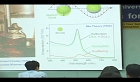
KCIPulse electroplating was studied to form nanocrystal structure effectively by changing plating current density and duty cycle. When both of plating current density and duty cycle are decreased from 100mA/㎠ and 70% to 50mA/㎠ and 30%, the P content ...
다국어 입력
あ
ぁ
か
が
さ
ざ
た
だ
な
は
ば
ぱ
ま
や
ゃ
ら
わ
ゎ
ん
い
ぃ
き
ぎ
し
じ
ち
ぢ
に
ひ
び
ぴ
み
り
う
ぅ
く
ぐ
す
ず
つ
づ
っ
ぬ
ふ
ぶ
ぷ
む
ゆ
ゅ
る
え
ぇ
け
げ
せ
ぜ
て
で
ね
へ
べ
ぺ
め
れ
お
ぉ
こ
ご
そ
ぞ
と
ど
の
ほ
ぼ
ぽ
も
よ
ょ
ろ
を
ア
ァ
カ
サ
ザ
タ
ダ
ナ
ハ
バ
パ
マ
ヤ
ャ
ラ
ワ
ヮ
ン
イ
ィ
キ
ギ
シ
ジ
チ
ヂ
ニ
ヒ
ビ
ピ
ミ
リ
ウ
ゥ
ク
グ
ス
ズ
ツ
ヅ
ッ
ヌ
フ
ブ
プ
ム
ユ
ュ
ル
エ
ェ
ケ
ゲ
セ
ゼ
テ
デ
ヘ
ベ
ペ
メ
レ
オ
ォ
コ
ゴ
ソ
ゾ
ト
ド
ノ
ホ
ボ
ポ
モ
ヨ
ョ
ロ
ヲ
―
http://chineseinput.net/에서 pinyin(병음)방식으로 중국어를 변환할 수 있습니다.
변환된 중국어를 복사하여 사용하시면 됩니다.
예시)
- 中文 을 입력하시려면 zhongwen을 입력하시고 space를누르시면됩니다.
- 北京 을 입력하시려면 beijing을 입력하시고 space를 누르시면 됩니다.
А
Б
В
Г
Д
Е
Ё
Ж
З
И
Й
К
Л
М
Н
О
П
Р
С
Т
У
Ф
Х
Ц
Ч
Ш
Щ
Ъ
Ы
Ь
Э
Ю
Я
а
б
в
г
д
е
ё
ж
з
и
й
к
л
м
н
о
п
р
с
т
у
ф
х
ц
ч
ш
щ
ъ
ы
ь
э
ю
я
′
″
℃
Å
¢
£
¥
¤
℉
‰
$
%
F
₩
㎕
㎖
㎗
ℓ
㎘
㏄
㎣
㎤
㎥
㎦
㎙
㎚
㎛
㎜
㎝
㎞
㎟
㎠
㎡
㎢
㏊
㎍
㎎
㎏
㏏
㎈
㎉
㏈
㎧
㎨
㎰
㎱
㎲
㎳
㎴
㎵
㎶
㎷
㎸
㎹
㎀
㎁
㎂
㎃
㎄
㎺
㎻
㎽
㎾
㎿
㎐
㎑
㎒
㎓
㎔
Ω
㏀
㏁
㎊
㎋
㎌
㏖
㏅
㎭
㎮
㎯
㏛
㎩
㎪
㎫
㎬
㏝
㏐
㏓
㏃
㏉
㏜
㏆

RISS 인기검색어

Effects of Electroplating Current Density and Duty Cycle on Nanocrystal Size and Film Hardness
한글로보기부가정보
다국어 초록 (Multilingual Abstract)
Pulse electroplating was studied to form nanocrystal structure effectively by changing plating current density and duty cycle. When both of plating current density and duty cycle are decreased from 100mA/㎠ and 70% to 50mA/㎠ and 30%, the P content in the Ni matrix was increased almost up to the composition of Ni3P compound and the grain growth after annealing was retarded as well. The as-plated hardness values ranging from 660 to 753 HV are mainly based on the formation of nanocrystal structure. On the other hand, the post-anneal hardness values ranging from 898 to 1045 HV, which are comparable to the hardness of hard Cr, are coming from how competition worked between the precipitation of Ni3P and the grain coarsening. According to the ANOVA and regression analysis, the plating current density showed more strong effect on nanocrystal size and film hardness than the duty cycle.
참고문헌 (Reference)
1 Mote1, V.D., "Williamson-Hall Analysis in Estimation of Lattice Strain in Nanometer-Sized ZnO Particles" 6 : 6-, 2015
2 McMahon, G, "Structural Transitions in Electroplated Ni-P alloys" 8 : 865-868, 1989
3 Lee, K.H, "Statistics Using EXCEL" JaYu Academy 2000
4 Ibl, N., "Some Theoretical Aspects of Pulse Electrolysis" 10 (10): 81-104, 1980
5 Chandrasekar, M.S, "Pulse and Pulse Reverse Plating-Conceptual, Advantages and Applications" 53 : 3313-3322, 2008
6 Koch, C.C, "Nanostructured Materials: Processing, Properties, and Applications" William Andrew Inc. 2007
7 Erb, U., "Nanostructured Materials: Processing, Properties, and Applications" William Andrew Inc. 235-292, 2007
8 선용빈, "Nano Crystalline Change by Heat Treatment" 한국반도체디스플레이기술학회 12 (12): 55-59, 2013
9 Wang, N., "Isokinetic Analysis of Nanocrystalline Nickel Electrodeposits upon Annealing" 45 (45): 1655-1669, 1997
10 Lu, K, "Grain Growth Kinetics and Interfacial Energies in Nanocrystalline Ni-P Alloys" 69 (69): 7345-7347, 1991
동일학술지(권/호) 다른 논문
-
- 한국반도체디스플레이기술학회
- 김경범
- 2015
- KCI등재
-
H.264/AVC를 위한 UEP Turbo Encoder
- 한국반도체디스플레이기술학회
- 김준
- 2015
- KCI등재
-
- 한국반도체디스플레이기술학회
- 김부종
- 2015
- KCI등재
-
- 한국반도체디스플레이기술학회
- 주강우
- 2015
- KCI등재
분석정보
인용정보 인용지수 설명보기
학술지 이력
| 연월일 | 이력구분 | 이력상세 | 등재구분 |
|---|---|---|---|
| 2027 | 평가예정 | 재인증평가 신청대상 (재인증) | |
| 2021-01-01 | 평가 | 등재학술지 유지 (재인증) | |
| 2019-01-01 | 평가 | 등재학술지 유지 (계속평가) | |
| 2016-01-01 | 평가 | 등재학술지 유지 (계속평가) | |
| 2012-01-01 | 평가 | 등재학술지 유지 (등재유지) | |
| 2010-03-25 | 학회명변경 | 한글명 : 한국반도체및디스플레이장비학회 -> 한국반도체디스플레이기술학회영문명 : The Korean Society of Semiconductor & Display Equipment Technology -> The Korean Society of Semiconductor & Display Technology | |
| 2010-03-25 | 학술지명변경 | 한글명 : 반도체및디스플레이장비학회지 -> 반도체디스플레이기술학회지외국어명 : Journal of the Semiconductor and Display Equipment Technology -> Journal of the Semiconductor & Display Technology | |
| 2009-01-01 | 평가 | 등재학술지 선정 (등재후보2차) | |
| 2008-01-01 | 평가 | 등재후보 1차 PASS (등재후보1차) |  |
| 2006-01-01 | 평가 | 등재후보학술지 선정 (신규평가) | |
학술지 인용정보
| 기준연도 | WOS-KCI 통합IF(2년) | KCIF(2년) | KCIF(3년) |
|---|---|---|---|
| 2016 | 0.29 | 0.29 | 0.26 |
| KCIF(4년) | KCIF(5년) | 중심성지수(3년) | 즉시성지수 |
| 0.21 | 0.18 | 0.217 | 0.02 |
연관 공개강의(KOCW)
이 자료와 함께 이용한 RISS 자료
나만을 위한 추천자료


